Introduction
In my 21 years of tracking semiconductor development, I’ve seen the industry progress from the ‘giant’ devices of 90nm to the atomic-scale 2nm wonders of 2027. I remember when a few million transistors on a chip seemed a marvel; today we’re putting billions of transistors.
As we discussed in reports on the [upcoming iPhone 18 Pro] and [Google Pixel 11 Pro Fold], 2nm silicon is the engine of the 2026-2027 era. Specifically, this leap in architecture provides the “Technical Bonus” needed to run native AI models. In this guide, I’ll explain the complex science behind 2nm technology in simple terms.
1. What Does “2nm” Actually Mean?
To understand this unprecedented progress, we need to consider its scale. Specifically, a nanometer is one billionth of a meter. Furthermore, a 2nm transistor is approximately the size of two strands of human DNA. This rapid miniaturization is the latest proof that Moore’s Law is still driving the industry forward, even as we approach the physical limits of silicon.
- The Technical Shift: Moving to 2nm technology makes it possible to fit more transistors in the same physical space. As a result, electrons have to travel a shorter distance, which increases processing speed and reduces power consumption.
2. From FinFET to GAAFET: The Architectural Leap
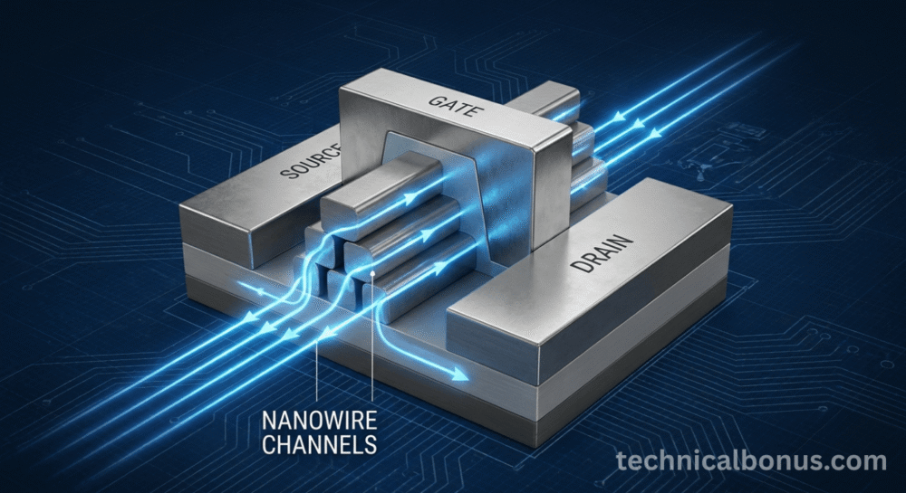
In addition, for years, the industry used ‘FinFET’ (Fin Field-Effect Transistor). In contrast, 2nm technology introduces GAAFET (Gate-All-Around FET).
- The Difference: In GAAFET, the gate is in contact with the channel on all four sides. This provides a significant “Technical Bonus” in power control, preventing the ‘leakage’ that used to cause heating problems in older 5nm or 7nm chips.
- This improved thermal control is why [Windows 12 Speed Tweaks] and [Smartphone Battery Guide] are much more effective on modern 2nm devices.
3. Why 2nm is the Backbone of 2027 AI
Moreover, as we analyzed in [Top 5 AI Productivity Tools] and [Cloud vs GPT Comparison], AI requires massively parallel processing.
- The 2nm process provides the high-density NPUs (neural processing units) needed to run these ‘agent-based’ models locally. Without this hardware breakthrough, [the future of technology in 2027] would still be dependent on slow, cloud-based processing.
4. Technical Comparison: The Evolution of Silicon
| Node Size | Architecture Type | Main Advantage |
| 7nm / 5nm | FinFET (Standard) | High-Performance Mobile |
| 3nm | Advanced FinFET | Early AI Integration |
| 2nm (2027) | GAAFET (Gate-All-Around) | Ultra-Efficiency & Local AI |
Conclusion: Beyond the Limits of Physics
Ultimately, we’re approaching the limits of silicon’s physical capabilities. 2nm technology represents one of the final frontiers of traditional computing. By understanding this science, you can discover why the hardware in your pocket today is truly a technological masterpiece. As industry leaders like [TSMC] continue to push the boundaries of semiconductor physics, the potential for our devices is limitless.
Disclaimer
This technical interpretation is based on the current 2026 semiconductor research and manufacturing roadmaps from TSMC, Samsung, and Intel. Every effort is made to simplify complex physics, however performance on end consumer hardware may vary. Expert insights are based on 21 years of tech industry observation.
